PCB layout design of DC-DC non isolated switching power supply
PCB lay
A common problem of switching power supplies is “unstable” switching waveforms. Sometimes, waveform jittering is so pronounced that audible noise can be heard from the magnetic components. If the problem is related to the printed circuit board (PCB) layout, identifying the cause can be difficult. This is why proper PCB layout at the early stage of a switching supply design is very critical. Its importance cannot be overstated.
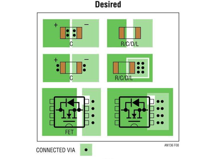
A good layout design optimizes supply efficiency, alleviates thermal stress, and most importantly, minimizes the noise and interactions among traces and components. To achieve these, it is important for the designer to understand the current conduction paths and signal flows in the switching power supply. The following discussion presents design considerations for a proper layout design for non-isolated switching power supplies.
Learn more →
About PWchip
COMPANY PROFILE
Wuxi PWChip Semi Technology CO., LTD., is an IC design house designs and manufactures analog and mixed-signal power management solutions in electronic systems.
Our vision is to offer customers the total power management solutions of superior quality, performance, service, and cost. With more than 15 years of analog power and discrete device experiences, we offer high performance design services with full technology coverage and process development capability.
Learn more →

